Global Thin Film Semiconductor Deposition Market Size, Share, Growth, Industry Statistic Report By Deposition Technology (Chemical Vapor Deposition (CVD), Physical Vapor Deposition (PVD)), Industry Vertical(IT & Telecom, Electronics, Energy & Power); By Regional Analysis (North America - U.S, Canada, Other) (Asia-Pacific - India, Japan, China, South Korea, Japan, Australia, and Other) (Europe - U.K., Germany, Netherlands, Lithuania, Austria, Belgium, Poland, Sweden, Spain, France, Russia and Other) (Middle East - Saudi Arabia, UAE and Africa - South Africa, Zimbabwe and RoW) - Global Industry Insights, Trends and Forecast, 2020-2027
Report Format : PDF
Published Date : Aug-2020
Pages : 174
Report ID : VSR007164
Report Format: PDF
Published Date: Aug-2020 | 174 Pages | Report ID: VSR007164
The Global Thin Film Semiconductor Deposition Market Size was valued at USD 16.54 billion in 2020 and is projected to reach USD xx.xx billion by 2027, at a CAGR of 14.01% during the forecast period. This report covers the forecast of the Thin Film Semiconductor Deposition market and its dynamics over the next 7 years, while also recognizing market application gaps, recent developments in the market, and high potential countries. Thin film semiconductors are the foils fabricated from artificial semiconductor materials with thickness ranging from nanometers to few hundred millimeters. The demand for thin film semiconductors has increased in the recent years due to their advantages such as higher efficiency, lightweight, less space consumption, and flexibility in shape as compared to conventional silicon (c-Si). They are widely used in various applications such as solar panels, DRAMs, microprocessors, and wearable technologies among others. The market is largely driven by the increasing demand of thin film solar panel and flexible electronics such as flexible display & batteries. Moreover, need for miniaturization of circuit had supplemented the growth of TFS deposition market. However, restraints associated with the TFS deposition market is huge initial investment required for setting up new manufacturing facility for TFS and increasing cost of raw materials. The market is analyzed on the basis of four regions, namely, North America, Europe, Asia-Pacific, and LAMEA.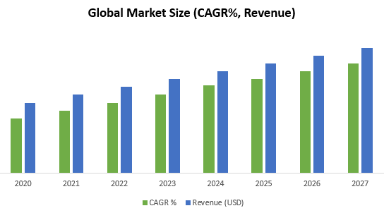
Veracious Statistics Research’s Report on Thin Film Semiconductor Deposition studies past and the current growth opportunities and trends to gain key insights of these indicators of the market over the forecast period from 2020 to 2027. For the period 2020-2027, the study offers revenue of the Thin Film Semiconductor Deposition market considering 2019 as the base year and 2027 as the forecast year. The compound annual growth rate (CAGR) for the market over the forecast period is also provided in the study.
Methodology:
The analysis of the report is carried on various primary and secondary data sources. The primary sources include conduction interviews with numerous industry analysts, suppliers, distributors, and other involved professionals. The secondary sources include a review of statistical data from press releases, government websites, annual reports of the companies, and other relevant documents.
During interviews, these primary and secondary sources provide exclusive information, which acts as a validation from global Thin Film Semiconductor Deposition market leaders. Access to an extensive internal repository and external proprietary databases helps this study to address questions and details regarding the market. Also, the report uses the top-down approach to assess the figures for each segment and to counter-validate them with the bottom-up approach.
We have covered two proprietary models in the Thin Film Semiconductor Deposition report, the FPNV Positioning Matrix and the Competitive Strategic Window and. The FPNV Positioning Matrix analyses players’ competitive marketplace in terms of product satisfaction and business strategy they follow to sustain in the market. In terms of applications, markets, and geographies, the Competitive Strategic Window analyses the competitive landscape.
Summarization of Report
The research report provides a perspective of the attractiveness of the regions and segments which are formulated based on their growth rate (CAGR) and market size. Leading analysts and industry professionals present in various regions have validated the data & information provided in the report. The report provides the detailed analysis of forecasted data, revenues, and major developments. It also offers crucial strategies adopted by major organizations catering to the Thin Film Semiconductor Deposition market. This provides important and in-depth insights to depict the overall market scenario.
Along with the market position, future trends, market share, market dynamics, opportunities, threats, risks and entry barriers, a detailed overview of the Thin Film Semiconductor Deposition market is included. In the form of graphs, tables, pie chart, and product figures, all the brief points and analytical market data are statistically pictured to provide users with overall information.
Also, the report sheds light on upstream raw materials, downstream client survey, marketing channels, industry development trends and recommendations that specifically provide useful information on major manufacturing equipment suppliers, raw materials suppliers, major distributors, and major consumers with their contact information, for Thin Film Semiconductor Deposition market chain analysis.
Growth Mapping
The key purpose of the report is to provide a growth map of the Thin Film Semiconductor Deposition market and hence assist the client's in the formulation of required strategies to meet the business goals. Thus, there are many qualitative and quantitative tools used for growth mapping of the market. These include PESTEL analysis for various regions involved in the market, SWOT analysis of the industry, PORTER'S five forces for determination of different attributes such as the power of the buyer and supplier engaged in the market, threat of substitution, intensity of competition and threat of the new entrants in the market.
Regional Analysis
The survey report includes a comprehensive investigation into the Thin Film Semiconductor Deposition Market, which is clearly arranged within the localities. The report provides an analysis for more than 20 countries of regional market players operating in the specific market, and results related to the target market. The report, which covers North America, South America, Europe, Asia Pacific (APAC), Africa and the Middle East, also contains a regional and country-level analysis of the market. The market is thoroughly analyzed in each region, allowing for the identification of regional market trends, impediments and opportunities for growth.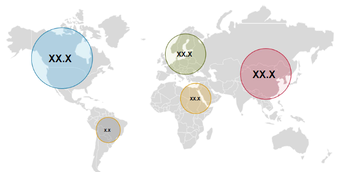
It is estimated that North America, the dominating country in Thin Film Semiconductor Deposition market will show considerable growth during the forecast period. The growth would be possible because of marketing analytics tools and because of existing players that are firmly established in the market since the beginning. In addition to that, government agencies, companies, third-party administrators, etc. are channelizing their efforts to make customer-centric products which will also contribute to the growth in this region. Rising demand, increased income, advanced technology and machinery, along with the programs for spreading the awareness of the need will likely cause the Thin Film Semiconductor Deposition market to grow substantially.
Asia-Pacific is supposed to have greater demand in the forecast year because of the fast-growing population. This factor alone stands out as the reason why the region will be dominating the Thin Film Semiconductor Deposition market share in the given forecast period. Due to improvements in GDP per capita and infrastructure development has urbanized the region to greater extent turning rural areas into urban areas. The sudden surge in the demand has caused the cities to fall into unsustainable consumption models. The top key players in the Thin Film Semiconductor Deposition market are located in the region.
As large projects are ongoing in countries like China, India, Japan, South Korea, Australia and Indonesia in Asia Pacific, the region has potential to bypass any competition. This is also because of the great amount of reserves that the region has. Exploration activities in China are increasing which is why China may have great demand for tin catalysts and compounds. According to the National Bureau of Statistics, Thin Film Semiconductor Deposition market will increase the regional demand during the forecast period.
As the major players in the Thin Film Semiconductor Deposition market focus on the expansion of the business throughout the globe, the regions like Middle East and Africa will experience steady growth. Latin America will experience considerable market growth because of the small-scale manufacturers attempting for a noteworthy share in the demand. On the contrary, Europe is said to show sluggish growth because of environment-centric regulation and it’s already developed countries.
Competitive Landscape
A competitive landscape for the Thin Film Semiconductor Deposition market is given in the study. To differentiate business attributes, key players operating in the industry have been identified and profiled. Company overview, latest trends, financial standings, and SWOT are some of the characteristics of key players in the industry that have been profiled in this study. Main players covered by the study on the global market are Applied Materials, Inc., Hitachi Kokusai Electric, Inc., Lam Research Corporation, Tokyo Electron Limited, Sumco Corporation, Oerlikon Balzers, ULVAC, IHI Hauzer Techno Coating B.V., CVD Equipment Corporation, Aixtron SE, and CVD Equipment Corporation among others.
The Report Provides Insights on The Following Pointers:
1. Market Development: Provides extensive information about emerging markets and analyzes the markets for the global Thin Film Semiconductor Deposition market.
2. Market Penetration: Offers detailed information provided by the key players in the global Thin Film Semiconductor Deposition market.
3. Competitive Assessment & Intelligence: Offers an exhaustive assessment of strategies, products, market shares and manufacturing capabilities of the leading players in the global Thin Film Semiconductor Deposition market.
4. Product Development & Innovation: Provides intelligent insights on future technologies, R&D activities, and new product developments in the global Thin Film Semiconductor Deposition market.
5. Market Diversification: Offers detailed information about recent developments, emerging geographies, new products launch, and investments in the global Thin Film Semiconductor Deposition market.
The Report Answers Questions Such As:
1. What is the global Thin Film Semiconductor Deposition market's competitive position?
2. What is the size of the Thin Film Semiconductor Deposition market globally?
3. What are the key factors driving the growth in the global Thin Film Semiconductor Deposition market during the forecast period?
4. What are the opportunities in the global Thin Film Semiconductor Deposition market?
5. Which are the main product fields to be invested in over the projected period in the global Thin Film Semiconductor Deposition market?
Enquiry for Table of Content
Global Thin Film Semiconductor Deposition Market Size, Share, Growth, Industry Statistic Report By Deposition Technology (Chemical Vapor Deposition (CVD), Physical Vapor Deposition (PVD)), Industry Vertical(IT & Telecom, Electronics, Energy & Power); By Regional Analysis (North America - U.S, Canada, Other) (Asia-Pacific - India, Japan, China, South Korea, Japan, Australia, and Other) (Europe - U.K., Germany, Netherlands, Lithuania, Austria, Belgium, Poland, Sweden, Spain, France, Russia and Other) (Middle East - Saudi Arabia, UAE and Africa - South Africa, Zimbabwe and RoW) - Global Industry Insights, Trends and Forecast, 2020-2027
Enquiry for Methodology
Global Thin Film Semiconductor Deposition Market Size, Share, Growth, Industry Statistic Report By Deposition Technology (Chemical Vapor Deposition (CVD), Physical Vapor Deposition (PVD)), Industry Vertical(IT & Telecom, Electronics, Energy & Power); By Regional Analysis (North America - U.S, Canada, Other) (Asia-Pacific - India, Japan, China, South Korea, Japan, Australia, and Other) (Europe - U.K., Germany, Netherlands, Lithuania, Austria, Belgium, Poland, Sweden, Spain, France, Russia and Other) (Middle East - Saudi Arabia, UAE and Africa - South Africa, Zimbabwe and RoW) - Global Industry Insights, Trends and Forecast, 2020-2027

Why Choose Veracious Statistics Research ?
Save Your Time
Cost-Effective Services
Wide Range of Reports
World Class Market Research
100% Customer Satisfaction
24/7 Customer care Support
Any more questions?
Get in touch with us quickly and easily. We are happy to help!
Do you still have questions?
Feel free to contact us anytime using our contact form.
Contact us

 2024 © Veracious Statistics Research All Rights Reserve